Home > MEMS / Microfabricated Products > Nanoimprint Mold > Nanoimprint Mold Custom

Nanoimprint mold custom

We respond to customer's unique specifications with our abundant achievements and accumulated technology and know-how

Contact us

Nanoimprint technology is being applied to various fields at an accelerating pace. We provide nanoimprint molds required in various steps of research, development, application, and commercialization.

We have been providing nanoimprint molds for more than 20 years as an application of semiconductor microfabrication technology. During this time, we have received guidance from many customers and have a wealth of experience in providing over 1000 molds.
We receive orders from universities, research institutes, companies, and customers in a wide range of fields such as semiconductors, optics, IT, bio, and medical.

Nanoimprint mold microfabrication technology and manufacturing know-how

■ Mold material

Materials such as quartz, silicon, SiC, and Ni can be specified according to the customer's nanoimprint.

■ Extremely fine

From minimum 20nm pattern to μm order. High aspect ratios are also possible.

■ Pattern

We can handle everything from repeated arrays of single patterns to complex patterns such as circuit patterns.

■ Multi-step pattern

We also offer multi-level stepped patterns for holograms, etc.

■ Three-dimensional shape

Various shapes such as minute microlens arrays (MLA), antireflection bodies (moth-eye structures), and inverted square pyramid patterns are processed.

■ High shape accuracy

The processing shape is also evaluated as a sharp edge. We also support tapered and reverse tapered microstructures by side wall control. Please contact us.

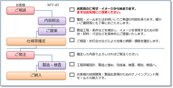
Flow of nanoimprint mold production request

Please feel free to contact us

Prior consultation is very important for custom molds. First of all, please contact us with your wishes and images. We will carefully respond to detailed consultations and questions.
 

Custom mold order flow

Custom mold Fine pattern processing example

This is an example of NTT-AT 's microfabrication of nanoimprint molds of various shapes and sizes. Please feel free to contact us regarding your desired pattern, substrate type, etc.

Ultra-fine pattern high aspect ratio pattern

Mold for nanoimprint Semi-custom ultra-fine pattern
36nm pitch dot

high aspect ratio pattern
aspect ratio 10

  • Substrate: quartz, silicon, SiO2/Si, Ni, SiC
  • Minimum pattern pitch: Approximately 35 nm (minimum pitch varies depending on the substrate and pattern.)
  • Depth: from 20nm
  • Patterns: L&S, dots, holes, rings
  • Substrate: Silicon
  • Pattern pitch: from 50nm
  • Depth: from 100nm
  • Pattern: Line, L&S
multilevel pattern V-groove type, blaze type pattern

multilevel pattern

8 level pattern

V-groove type, blaze type pattern

1 μm pitch V groove

  • Substrate: quartz, silicon, SiO2/Si, Ni electroforming
  • Minimum pattern: from 250nm
  • Number of levels: Up to 8 levels
  • Level depth: from 50nm
  • Total depth: up to 20μm
  • Substrate: Silicon
  • Pattern pitch: from 100nm
  • Depth: from 50nm
Conical pattern (Moth-eye structure) Spherical pattern (microlens)

Conical pattern (Moth-eye structure)

8 level pattern

Spherical pattern (microlens)

1 μm, zag 0.3 μm

  • Substrate: Quartz, Ni electroformed
  • Pattern pitch: from 200nm
  • Depth: 100 to 1000nm
  • Array: square array, triangular array, random array
  • Substrate: quartz, silicon, SiO 2 /Si, Ni electroformed
  • Pattern pitch: 1 to 250nm
  • Shape: Spherical
  • Array: square array, triangular array, random array
quadrangular pyramid pattern Fukahori Pattern

quadrangular pyramid pattern

square pyramid pattern array

Fukahori Pattern

40 μm height cylindrical pattern

  • Substrate: Silicon
  • Pattern pitch: from 500nm
  • Depth: from 300nm
  • Substrate: Quartz
  • Depth: up to 100 μm


Product Line

close up

Service list

close up

List of proposals for problem solving

close up

Catalog list

close up