
Feature
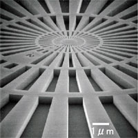
X-ray chart SEM image
X-ray microscopy is applied as a high-resolution imaging method in various fields, but charts with sufficiently high resolution are required for evaluation. NTT-AT 's X-ray chart, which has a high-definition tantalum (Ta) absorber pattern formed on SiC and SiN membranes, is used for resolution evaluation at synchrotron radiation facilities around the world.
Depending on your application, you can choose from three types: standard type, thick film high resolution type, and ultra high resolution type. We also offer reflective charts for the EUV region.
Depending on your application, you can choose from three types: standard type, thick film high resolution type, and ultra high resolution type. We also offer reflective charts for the EUV region.
Standard product specifications
| item | Standard type XRESO-100 |
Thick film high resolution type XRESO-50HC |
Super high resolution type XRESO-20 |
|
|---|---|---|---|---|
| pattern | Absorber | Ta, 1.0 µm thickness | Ta, 500 nm thickness | Ta, 100 nm thick |
| minimum dimension | 100nm | 50 nm | 20 nm (radial pattern) | |
| pattern area | 250 µm×350 µm |
300 µm×300 µm
|
||
| membrane | Ru (20 nm)/SiN (2 µm) | Ru (20 nm)/SiC (200 nm)/SiN (50 nm) | ||
| substrate | Material/outer shape | Si, 10 mm×10 mm | ||
| Thickness | 1 mm | 0.625 mm | ||
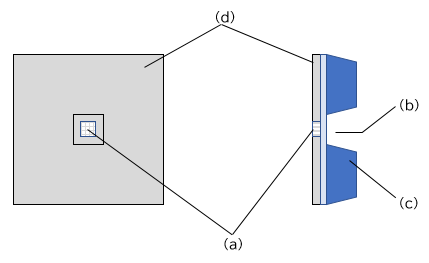
(a) X-ray chart (b) Ru/SiN membrane (c) Si substrate (d) Ta absorber
*The specifications listed are subject to change without notice for product improvement. please note that.
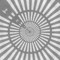
Representative pattern SEM image
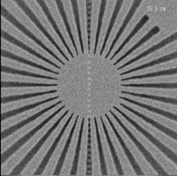
radial pattern
(XRSO-20)
(XRSO-20)
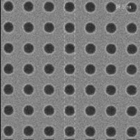
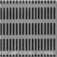
100 nm hole pattern
(XRESO-20)
(XRESO-20)
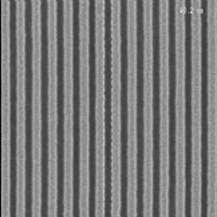
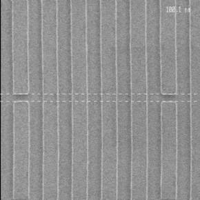
50 nm line & space pattern
(XRSO-20)
(XRSO-20)
50 nm line & space pattern
(XRESO-50HC)
(XRESO-50HC)
pattern layout
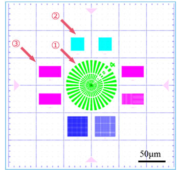
Super high resolution type XRESO-20
①Radial pattern, ②100 nm hole pattern, ③50 nm line & space pattern
①Radial pattern, ②100 nm hole pattern, ③50 nm line & space pattern
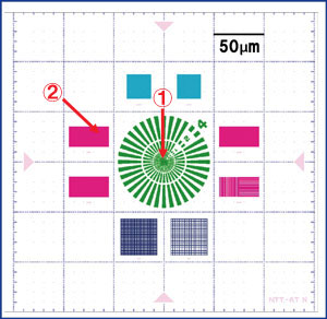
Thick film high resolution type XRESO-50HC
①Radial pattern, ②50 nm line & space pattern
①Radial pattern, ②50 nm line & space pattern
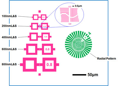
Standard type XRESO-100
Imaging example
Inspection equipment: Token TUX-5000F, chart: XRESO-50HC
(Courtesy of Token Co., Ltd.)
(Courtesy of Token Co., Ltd.)
Custom chart manufacturing example
Reflective chart for EUV
Multilayer film: Mo/Si for wavelength 13.5 nm, absorber: Ta
Multilayer film: Mo/Si for wavelength 13.5 nm, absorber: Ta
Download materials
| X-Ray Chart Related Bibliography (English) | 183KB | download |
|---|
Please contact us
Please feel free to contact us for inquiries such as an estimate.
 close up